visual
SCROLL
introduction
The technology of packaging and testing
an integrated circuit while at the wafer level, WLCSP
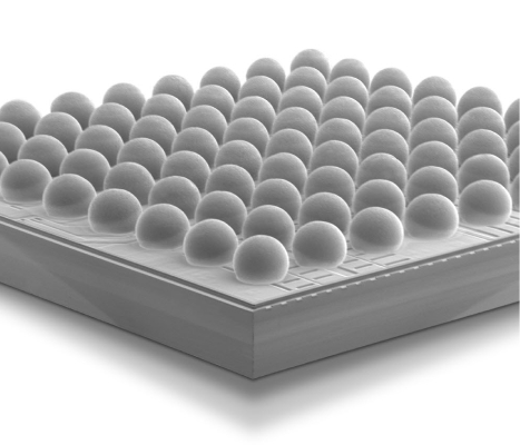
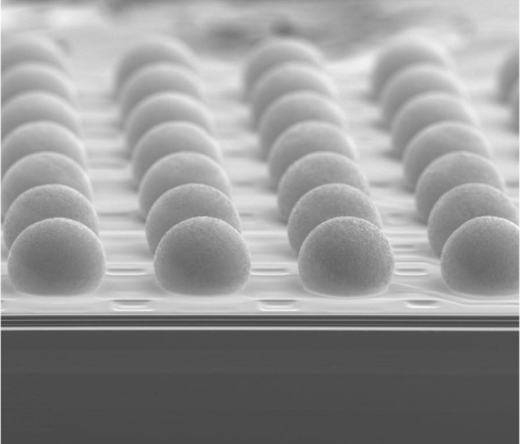
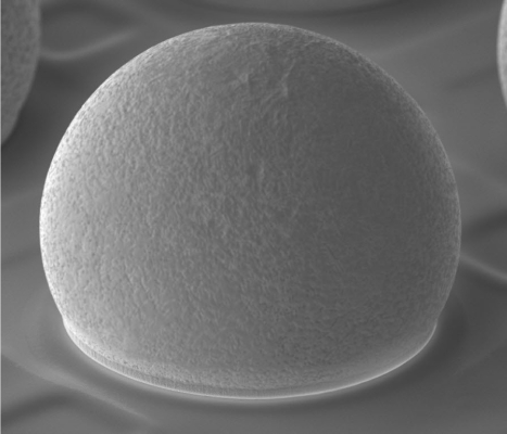
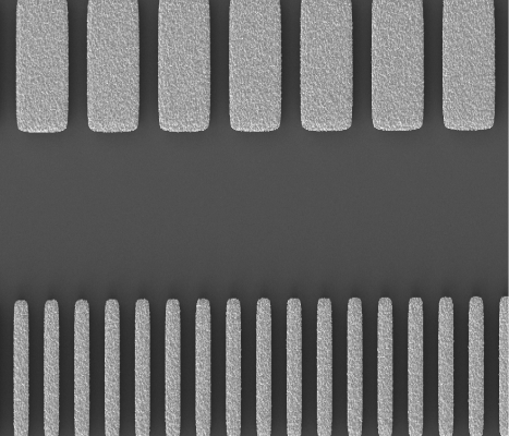
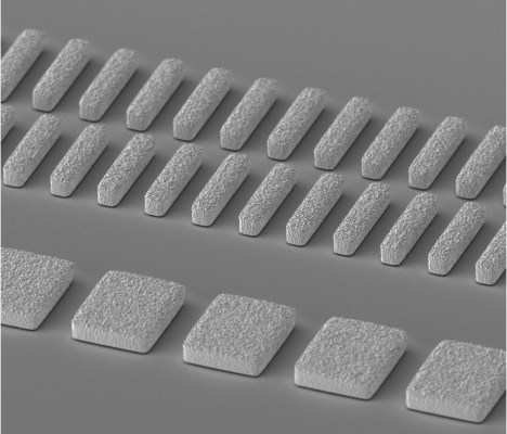
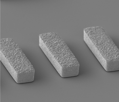
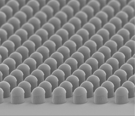
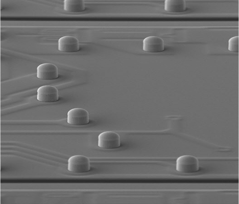
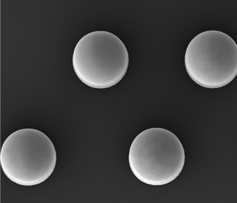
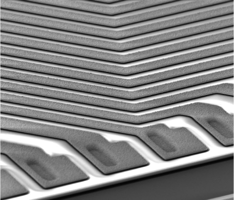
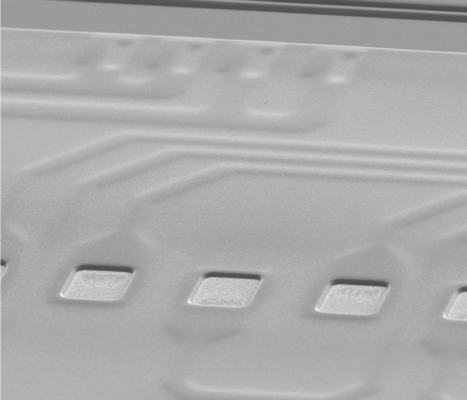
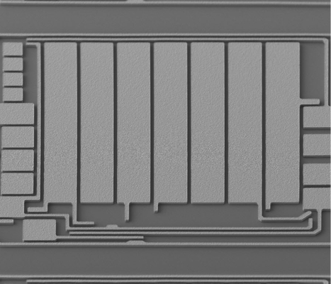
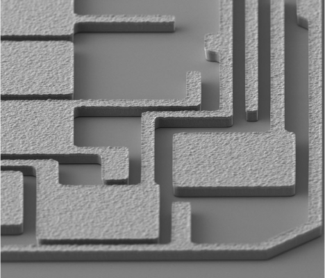
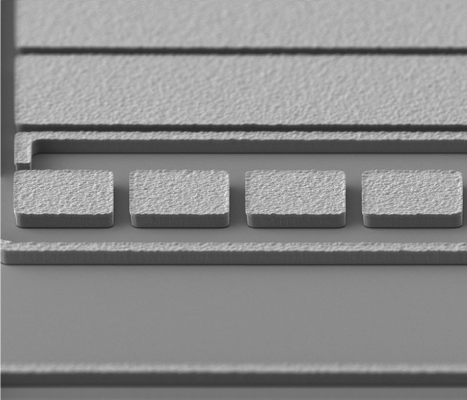
Wafer-level Packaging (WLCSP) is the technology of packaging and testing an integrated circuit while at the wafer level and then slicing it into chips to make the completed product, which differs from the conventional method of slicing the processed wafer first into individual chips and then packaging them. WLCSP is a true chip-scale packaging technology. Demand for WLCSP is increasing rapidly in the mobile market, due to the realization of a true chip-scale package with excellent electrical properties and price competitiveness. The WLCSP continues to expand its scope of application. LB Semicon currently provides various layers of WLCSP solutions ranging from two layers to six layers tailored to meet the needs of our customers.
Application
-

PMIC
-

RF & BB SoC
-

Transceiver
-

AOC
-

Sensors
Process Capability
-
Bumping
-
01.
8inch and 12inch Available
-
02.
WLCSP Structural Option
- 1P1M
- 2P2M (Single RDL with UBM)
- 3P3M (Dual RDL)
-
03.
Ball Pitch
- 0.3, 0.35, 0.4, 0.5mm
-
04.
Ball Height
- Ball drop : > 0.15mm
- Electroplated : < 0.11mm (Lead free, SnAg 1.8%)
-
05.
Re-PSV Material Option
- High temperature curable Polyimide
- Low temperature curable Polyimide
-
06.
Re-PSV Thickness
- 5 to 20um
-
07.
Re-PSV Opening Diameter
- Min. diameter : 25um
-
08.
RDL Thickness
- 3 to 10um (20um under development)
-
09.
RDL Width / Space (min)
- 12/12um
-
01.
-
Backend
-
01.
Back-Grinding for Wafer Thinning (min)
- >150um
-
02.
Backside Coating
- Available
-
03.
Scribe Lane for Dicing (min)
- 60um (Laser Grooving Available_80um)
-
04.
Die size (min) available for TnR
- 0.5x0.5mm
-
05.
Inspection
- Post Sawing AOI, 6side Inspection @ TnR
-
01.
introduction
Gold Bumped, thin and lightweight packages with high I/O and flexible interconnection, Au Bump
Gold bumped wafers are in general applied on packages such as COG (Chip on Glass), COF(Chip on Film), COP(Chip on Plastic), primarily for consumer products. This technology was developed as an alternative to the wire bonding technology. The gold bumped chip will be mounted on the package through the thermal compression method. As demand is increasing for thin and lightweight packages with high I/O and flexible interconnection, these gold bumped wafers will represent a suitable solution for such products as mobile devices.
Application
-

COF and COG PKG for TV
-

Monitor
-

Notebook DDIC
-

Mobile
-

Tablet
-

Automotive DIC
Process Capability
-
Au Bumping
-
01.
8inch and 12inch Available
-
02.
Various Hardness Available from 50Hv Up to 90Hv
-
03.
Bump Height (Typical)
- 8 to 16um
-
04.
Height Uniformity
- WID : ≤ 2um
- WIW : ± 2um
-
05.
Bump Pitch (min)
- Straight 21um
-
06.
BOA(Bump On Active circuit) Structure Qualified
-
07.
2D, 3D AOI
-
01.
introduction
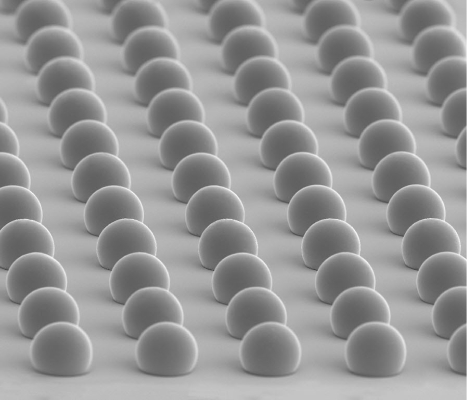
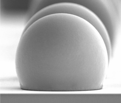
applied on various flip chip packages such as COC, fcBGA and fcQFN, Solder Bump
solder bump is being applied on various flip chip packages such as COC, fcBGA and fcQFN. LB Semicon currently provides a Lead-free solder bump solution based on a fine pitch structure, and even for the products such as wafers designed for QFN purpose that are not suitable for flip chip packages because of the pad position. Flip chip packages can still be applied without changing their pad layout with the help of the RDL process.

Application
-

fcBGA PKG for AP
-

SoC
-

PMIC
-

Graphics
Process Capability
-
Bumping
-
01.
8inch and 12inch Available
-
02.
Solder Bump Structural Option
- 1M (Direct Solder Bump on Fab-Passivation)
- 1P1M (Solder Bump on Polymeric Re-Passivation)
- 2P2M (Solder Bump with Electroplated Cu RDL)
-
03.
Solder Bump Pitch and Height
- Bump Pitch (min) : 140um
- Bump height : 50 to 110um (Depending on Bump Diameter and Pitch)
-
04.
Solder Material Option
- Lead Free SnAg (Ag1.8wt%)
-
05.
Re-Passivation Option
- High Temperature Curable Polyimide
- Low Temperature Curable Polyimide
-
01.
introduction
Developed to meet such needs for fine pitches(40um or smaller), is currently being applied to various packages, Cu Pillar bump
As semiconductor devices are rapidly becoming more integrated and faster, chip’s I/O density is increasing at a rapid pace while the bump pitch is continuously decreasing. Cu pillar is a bumping technology, developed to meet such needs for fine pitches, and it can accomplish much finer pitch of 40um or smaller, compared to the 150um level that existing Solder bumping method could reach. Cu pillar is currently being applied to various packages and its application will be expanded even more because of its excellent thermal dissipation performance and electro-migration properties, compared to Solder bumping.
Application
-

fcBGA and fcQFN PKG for RFIC
-

BB & AP Processor
-

Power Amplifiers
-

NAND Flash
-

WiFi Module
Process Capability
-
Bumping
-
01.
8inch and 12inch Available
-
02.
Cu Pillar Structural Option
- 1M (Direct CuP on Fab-Passivation)
- 1P1M (CuP on Polymeric Re-Passivation)
- 1P2M (Both RDL First and PI First Available)
- 2P2M (CuP with Electroplated Cu RDL)
-
03.
Cu Pillar Pitch and Height
- Pitch (min): 50um Pitch for 8inch / 40um Pitch for 12inch
- Total CuP Height : 30 ~ 90um (Depending on Cu Pillar Diameter and Pitch)
-
04.
Cu Pillar Material Stack-up Option
- Cu Post / Solder Cap
- Cu Post / Ni Barrier Metal / Solder Cap
-
05.
Solder Cap Material Option
- Lead Free SnAg (Ag1.8wt%)
-
01.
introduction
accomplishes SIP by repositioning the layout of the I/O pad, Au RDL
Au RDL is mostly used to reposition the layout of the I/O pad so that the product becomes suitable for the wire bonding package. Au RDL provides an excellent wire bond-ability and high reliability, and it accomplishes SIP by repositioning the layout of the I/O pad in a way that makes it possible to apply a stack die wire bonding more easily without the pad layout design changes of memory devices.
Application
-

Mostly used for Multi stack Wire bonding PKG for Memory such as NAND Flash and DRAM
-

Available for all applications that need Au wire bonding
Process Capability
-
Bumping
-
01.
8inch and 12inch Available
-
02.
Au RDL Structural Option
- 1P1M (Au RDL on Polymeric Re-Passivation)
- 2P1M (Additional Polymeric Re-Passivation Over RDL)
-
03.
Au RDL Thickness
- 3 to 5um by Electroplating
-
04.
Au RDL Width / Space
- 15 / 15um
-
05.
Re-Passivation
- Low Temperature Curable Polyimide
-
01.
introduction
a layer is formed directly on the fab passivation without additional lower polymer protective layers, Thick Cu
In the thick Cu process, a layer is formed directly on the fab passivation without additional lower polymer protective layers. Due to low resistance of copper, this process provides a higher current efficiency compared to the general aluminum wiring, and the thick copper layer could absorb a significant amount of stress during the bonding process to ensure a wider bonding process window, and the use of various wires such as Au, pure and Pd/Cu wires allowing a BOAC process in a stable manner without worrying about cracks. * BOAC : a layout technology called “Bond Over Active Circuit”
Application
-

Wire bonding PKG for Power Management IC and Memory
Process Capability
-
Bumping
-
01.
8 inch Available
-
02.
Thick Cu Structural Option
- 1M (Direct Thick Cu on Fab-Passivation)
- 1P1M (Direct Thick Cu + Additional Polymeric Re-Passivation Over Thick Cu)
- 1P1M (Thick Cu on Polymeric Re-Passivation)
-
03.
Thick Cu Thickness
- 5 to 10um
-
04.
Thick Cu Stack-up Material : Electroplated Cu/Ni/Au
- Cu for Rs Reduction
- Ni for Diffusion Barrier
- Au for Wire Bonding ( Au and Cu Wire Bonding Available)
-
05.
Thick Cu Width / Space
- 12/12um
-
06.
Re-Passivation Option
- High Temperature Curable Polyimide
- Low Temperature Curable Polyimide (Under Qualification)
-
01.
introduction
Bonding technology that directly connects the Driver IC with conductive bumps onto the glass panel, COG
COG is an abbreviation of Chip On Glass, and it is a bonding technology thatdirectly connects the driver IC with conductive bumps on the glass panel, and is applied to high resolution LCD and OLED products.
Process
-
01
Laminating
A process where protective tapes are bonded to the patterned surface to protect the circuit side of a wafer and prevent wafer broken when Wafer Grinding
-
02
Back Grinding
A process where the backside of the wafer is polished with blade wheels to meet our customers’ needs for low profile and small form factor products
-
03
Laser Marking
A process where each chip is laser etched with a unique identification code to trace each of them
-
04 Option
Laser Grooving
A process of removing the low-K layer and metal layer, which are difficult-to- cut-materials, using a laser.
-
05
SAW
A process of cutting the tape mounted wafer into individual chips based on the prescribed chip size
-
06 Option
Plasma
A process where dust particles on wafer surfaces are eliminated using plasma
-
07
Post AVI
A process where surface damage is inspected after chipping
-
08
UV Irradiation
A process where the adhesive strength of UV tapes is weakened for a smooth pickup
-
09
Pick & Place
A process where only good quality chips from wafers that went through a sawing process are selectively transferred to the trays
-
10
AVI
A process where chips transferred to trays are visually inspected
-
11
Visual Inspection
A process where the good quality chips transferred to chip carriers or trays are subject to the pass/fail discrimination in accordance with visual inspection standards
-
12
Packing
A process where the good quality chips that have gone through the final selection process are subject to a series of packing including vacuum packing, inner packing and outer packing
introduction
The technology of packaging and testing an integrated circuit while at the wafer level, WLCSP
Process
-
01
Laminating
A process where protective tapes are bonded to the patterned surface to protect the circuit side of a wafer and prevent wafer broken when Wafer Grinding
-
02
Back Grinding
A process where the backside of the wafer is polished with blade wheels to meet our customers’ needs for low profile and small form factor products
-
03
Back Side Coating
A process of applying a special film on the back of the wafer to protect the chip from external impact
-
04
Laser Marking
A process where each chip is laser etched with a unique identification code to trace each of them
-
05
Foil Mount
A process where frames and wafers are bonded together using tapes to facilitate a sawing process
-
06 Option
Laser Grooving
A process of removing the low-K layer and metal layer, which are difficult-to- cut-materials, using a laser
-
07
SAW
A process of cutting the tape mounted wafer into individual chips based on the prescribed chip size
-
08
Post AVI
A process where surface damage is inspected after chipping
-
09
UV Irradiation
A process where the adhesive strength of UV tapes is weakened for a smooth pickup
-
10
Tape & Reel
A process where only good quality chips from wafers that went through a sawing process are selectively transferred to the reels
-
11
Visual Inspection
A process where the good quality chips transferred to chip carriers or trays are subject to the pass/fail discrimination in accordance with visual inspection standards
-
12
Packing
A process where the good quality chips that have gone through the final selection process are subject to a series of packing including vacuum packing, inner packing and outer packing
introduction
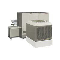
The Process of checking the status of each chip through various inspections at wafer level,
Chip Probe Test
The EDS (Electrical Die Sorting) process conducted by LB Semicon is a process that checks whether the quality characteristics of individual chips have reached the target level. It is operated to improve the work efficiency of subsequent processes by sorting out good/defective chips, correcting problems in the design stage, and sorting out defective chips in advance. We classify the device type according to the purpose of the semiconductor chip and perform electrical performance and quality inspection of the chip using a dedicated tester suitable for each chip's characteristics. In this process, the Auto Wafer Prober can be used to automatically, safely and quickly test individual chips. The tests can be categorized into three types: temperature, speed, and operation tests. Temperature tests are applied and tested by conditions from low temperature (Cold, -40℃) to high temperature (Hot, 125℃) because they must be operated in various temperature environments when actual chips are used. Speed tests measure the operating speed of the products. the operating speed of the semiconductor itself is important, but the communication speed with peripheral devices is also important, so it is vital to test the speed in various environments that meet the specifications of the chip. Operation tests include DC, AC, and function tests, and each test verifies current or voltage, analog characteristics, and operational status of each chip.
-
01 IAQ
-
02 P-TEST
-
03 INKING
-
04 SCOPE V/I
-
05 DOC.
INSPECTION -
06 QC GATE
(OGI) -
07 PACKING
(QPI) -
08 Shipping &
Back-end
-
 DDI Test System
T6372 / T6373 / T6391 / T6391S
-
 DDI Test System
TS670 / ST6730A / ST6731A
-
 PMIC Test System
T2000-IPS / ETS-364B
-
 CIS Test System
T2000-ISS
-
 SoC Test System
Ultra-FLEX
Features
화면을 좌우로 스와이프하여 확인하여 주세요.| Application | Vendor | Model |
Specification (Pin mux, Pattern mux) |
Remark |
|---|---|---|---|---|
| DDI | Advantest | T6372(ND2) | 437.5MHz | - |
| T6373(ND3) | 437.5MHz | HSIF : 1.25GHz | ||
| T6391(ND4C) | 800MHz | UHSIF : 1.35GHz ~ 2.0GHz(License) | ||
| T6391S(ND4ST) | 800MHz | UHSIF : 2.0GHz ~ 3.25GHz(License) | ||
| Yokogawa | TS670 | - | UVI : 2.0A | |
| ST6730A | 375MHz | NSIO | ||
| ST6731A | 1.25GHz | GSIO | ||
| PMIC | Eagle | ETS-364B | 66MHz | - |
| Advantest | T2000-IPS | 250MBps | - | |
| T2000-IPS/EPP | 250Mbps/800Mbps/1Gbps | - | ||
| T2000-IPS 52TH | 1Gbps | GPWGD | ||
| CIS | Advantest | T2000-ISS/32 | 800Mbps | 1.2G Capture Module |
| T2000-ISS/64P | 1Gbps | 4.8G Capture Module | ||
| SOC | Teradyne | Ultra-FLEX | 1600Mbps | - |
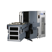
Re-configuration Process
We provide a process solution that allows a wafer level chip test while minimizing losses, for the cases where sorting issues are raised or Test Program Debugging needs to be retested for chips after the sawing process.
- Chip on Tray
- Chip on Blue Tape(Ring Frame)
- Re-Test
- 2200 evo-Key Features(Re-con)
- Specifications FP 3000(Test)
